Controlling the energy band alignment/offset via epitaxially well-defined heterostructures is a ubiquitous solution for manipulating charge carriers in optoelectronics. Single p-n junctions are the foundational elements for much of today’s semiconductor technology. Double heterostructures allow efficient carrier injection, low voltage operation, and increased output/performance; and have enabled semiconductor lasers and LEDs among many devices. Our recent efforts have focused on introducing structurally and electronically well-defined active heterojunctions within colloidal nanorods through versatile solution chemistry. By doing so, one can combine the benefits of conventional semiconductor heterostructures with size and shape dependent properties of nanocrystals. More importantly, we have demonstrated that new capabilities can arise in these materials. Various motifs of epitaxial heterojunctions introduced in nanorods have led to, for example, optical anisotropy and unusual shapes and lattice strain effects that are not accessible in thin films or bulk materials. Our efforts on studying photophysics and carrier dynamics of these nanorod heterostructures along with developing unconventional means of integrating them into light detecting, harvesting and emitting devices are leading to new engineering paradigms for next-generation optoelectronics and photovoltaics.
Double Heterojunction Nanorods (DHNRs) for Multifunctional Optoelectronics
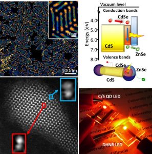 The double heterostructure is one of the most important components of today’s optoelectronic devices. It consists of a smaller band gap semiconductor sandwiched between two larger band gap materials. The outer layers allow independent control over injection/extraction/blocking of electrons and holes to the “active” center. In the thin film geometry, the substrate breaks the symmetry and sequential growth can easily lead to the smaller gap material in contact with both outer layers that are properly oriented for electrical contacts. In the solution synthesis of colloidal nanocrystals, the thermodynamic driving force to minimize surface-to-volume ratio often leads to nearly spherical shapes and makes such a geometry difficult to achieve. Core/shell/shell structures can take the form of double heterostructures but will have only one component physically accessible, making them undesirable for most optoelectronic applications. To overcome this challenge, we have exploited directional growth of nanorods to achieve double heterojunction nanorods (DHNRs). Here, a seed nanorod acts as the first outer layer, the “inner” smaller gap material is grown at the tips of the seed, and the second outer layer is selectively grown as a shell around these tips . We have demonstrated usefulness of these DHNRs as electroluminescent materials in LEDs where the double heterostructure designed into the nanorods allows not only the benefit of improved carrier injection/blocking but also transition dipole orientation that enhances light outcoupling . These DHNR-LEDs exhibit one of the highest luminous power efficiencies for LEDs fabricated by all solution processing, even rivaling or surpassing vacuum-deposited OLEDs. Most recently, we are working on developing multifunctional optoelectronics using DHNRs that could open up novel applications in displays, lighting, energy harvesting and data communication.
Nanorod Heterostructures for Charge Separation
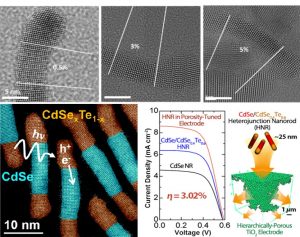 Materials that can efficiently separate photoinduced charges are at the heart of photovoltaics and photocatalysis. Anisotropic heterostructures of semiconductor nanocrystals with well-defined composition and structure provide an interesting platform to examine how size, shape, composition and even lattice strain can affect heterojunctions’ ability to separate charges. To this end, we have developed colloidal nanorod-based heterostructures with variable composition, geometry and lattice strain. Interestingly, by varying how or where the second phase grows on a seed nanorod, unusual and unexpected structures have been achieved. For example, starting from Cu2-xS nanorods, we have shown that varying the degree of cation exchange vs. catalytic growth can lead to heterostructures with unique shapes. The effects of growth location is exemplified in CdSe/CdTe nanorod heterostructures which can have very little lattice strain effects when CdTe is grown at the tips whereas side growth can cause large anisotropic strain (~5% compression) leading to extreme bending of otherwise a highly brittle material. Our efforts on elucidating carrier dynamics in these materials have shown that both composition and lattice strain can alter charge separation rates across heterointerfaces by almost an order of magnitude. We have also demonstrated that these nanorod heterostructures can be used as efficient charge separation centers in solar cells, leading to one of the highest power conversion efficiencies for nanorod-sensitized devices. Efforts are ongoing to further elucidate reaction mechanisms that lead to uniquely strained materials and to develop photovoltaics with unusual device formats (e.g., flexible, conformable to curved surfaces, etc.) that can extend the use of solar cells to unconventional settings.