Google Scholar
[2021][2020][2019][2018][2017][2016] [2015] [2014] [2013] [2012] [2011] [2010] [2009] [2008] [2007] [2006] [2005] [2004] [2003] [1997-2002]
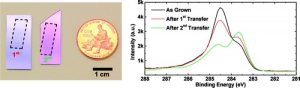
- S. Unarunotai, J. C. Koepke, C. –L. Tsai, F. Du, C. E. Chialvo, Y. Murata, R. Haasch, I. Petrov, N. Mason, M. Shim, J. Lyding, J. A. Rogers, “Layer-by-Layer Transfer of Large Area Sheets of Graphene Grown in Multilayer Stacks on Single SiC Wafer,” ACS Nano 4, 5591 – 5598 (2010). [DOI: 10.1021/nn101896a]
- M. Shim and H. McDaniel, “Anisotropic Nanocrystal Heterostructures: Synthesis and Lattice Strain,” Curr. Op. Sol. State Mater. Sci. 14, 83 – 94 (2010). Invited review article. [DOI: 10.1016/j.cossms.2010.04.001]
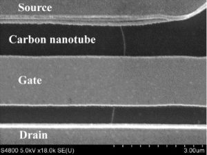
- S. Kim, S. Kim, D. B. Janes, S. Mohammadi, J. Back, and M. Shim, “DC Modeling and the source of flicker noise in passivated carbon nanotube transistors,” Nanotechnology 21, 385203 (2010). [DOI: 10.1088/0957-4484/21/38/385203]
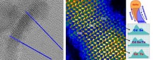
- H. McDaniel, J. –M. Zuo, and M. Shim, “Anisotropic Strain Induced Curvature in Type II CdSe/CdTe Nanorod Heterostructures,” J. Am. Chem. Soc. 132, 3286 – 3288 (2010). [DOI: 10.1021/ja910233a]
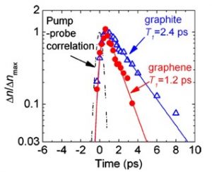
- K. Kang, D. Abdula, D. G. Cahill, and M. Shim, “Lifetimes of optical phonons in graphene and graphite by time-resolved incoherent anti-Stokes Raman scattering,” Phys. Rev. B 81, 165405 (2010). [DOI: 10.1103/PhysRevB.81.165405]
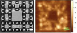
- K. H. Hsu, J. H. Back, K.-H. Fung, P. M. Ferreira, M. Shim, and N. X. Fang, “SERS EM-field Enhancement Study through Fast Raman Mapping of Optical Sierpinski Carpet Fractals,” J. Raman Spectr. 41, 1124 – 1130 (2010). [DOI:10.1002/jrs.2581]